DV BMU Emissions Test Issues
During development of our Battery Management Unit (BMU) we performed DV testing and found an issue in the radiated emissions test. Our schedule to meet the customers deadlines was tight so we did not perform pre-DV emissions scans which would have caught this failure earlier. We had to find a solution quickly to keep the BMU project on schedule so we needed to narrow down the root cause of the emissions failure, find a workable solution and test a prototype fix all within < two weeks? >.
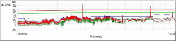
Figure 1 – BMU measured emissions (Peak, QP and Average) and corresponding limits
 We quickly found the root cause of the emissions issue; using a near field magnetic field probe along with OpenECU’s spectrum analyzer our engineers found that the emitted noise was due to the SPI isolator integrated circuit (IC). That IC transfers the serial peripheral interface (SPI) signals and DC power from the 12V vehicle side of the BMU to the high voltage battery side for acquisition of the high voltage measurements such as the battery stack voltage. This device has internal transformers which transfer the power and signals across a 2500V isolation barrier. This requires high frequency switching to provide high efficiencies in the transformers. Switching noise internal to this part was being inserted into the high voltage side of our module and radiating out into the environment.
Dana engineers worked with the manufacturer of the isolator IC, Analog Devices Incorporated (ADI), to investigate the source of its noise. ADI engineers developed a reference design for this part that could pass automotive emissions tests but had found similar issues during their initial reference design work.
ADI engineers found that a capacitive current path was required to bypass the high frequency noise of the isolated DC/DC convertor back from the high voltage side of the board to the low voltage side. Also, filtering was required between the 5-volt isolated output of the device to the devices it powers on the high voltage side. ADI engineers recommended extending copper internal to the circuit board across the isolation barrier to provide an overlapping capacitive path. Our customer did not want to us to implement this approach because their research had indicated the possibility of breakdown of the isolation material in the printed circuit board over long-term use. Dana engineers modified a board to add high voltage rated capacitors across the isolation barrier along with filtering of the power output from the device.
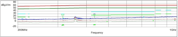
Retesting the module for emissions indicated that these changes had reduced the noise below the acceptance levels of the test. Unfortunately, the re-test found that now the module was failing the test for susceptibility to the external noise. Dana engineers investigated this and realized that when the filtering to the power supply was added, the output impedance was increased to the point that the bypassing capacitance on the high voltage measurement parts was inadequate to overcome the injected noise a certain frequencies. Dana engineers calculated what capacitance was required, added the capacitors to the modified module and went back for another day of testing. This round the module passed the tests. A design with these modifications was ready for release with hours to spare before causing a schedule slip for the customer.
Dana recommends a project schedule includes a suite of pre-design verification tests which can be done at a reduced cost in time and money in development schedules. In this project these tests were not planned in order to meet an aggressive schedule and issues that the pre-DV testing would have found were not found until the DV testing. Fortunately, Dana engineers were able to find the source of the problem and a solution without causing a slip in the project schedule.
 Accessibility